How is monocrystalline silicon made?
info
Solar panel technology – the key for preserving our planet
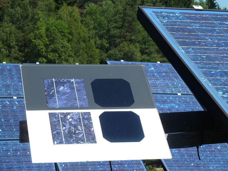
There is no secret for anyone that the sun is an extremely powerful source of renewable energy for us. As the non-renewable resources are becoming more and more limited for the humanity’s needs, it’s no surprise that research teams around the world are focusing on developing new technologies to harness the power of renewable energy resources like the sun.
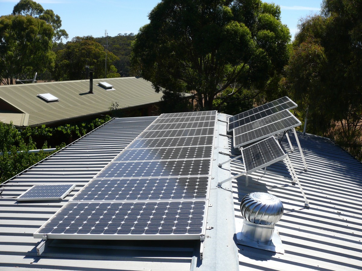
When it comes to sun energy saving we cannot miss the technology of solar panels which has been growing in popularity in the past decades. Monocrystalline solar panels have become the standard choice for solar energy panels.
Why monocrystalline silicon is the most preferred material for modern solar panels?
Before describing in detail the process of manufacturing monocrystalline solar panels let’s take a look at exactly what monocrystalline is.
Monocrystalline is the main material used for silicon chips which are applied in basically all modern electronic equipment that exists today.
The main application of monocrystalline is in the production of solar cells. It plays a role as a photovoltaic material with light-absorbing abilities used in the manufacturing process of solar cells.
Although its production process is more time-consuming and relatively expensive, it is a preferred option for its amazing electronic properties.
Its main ingredient is silicon which has continuous crystal lattice whose edges are unbroken and it doesn’t have any grain boundaries. Monocrystalline silicon is manufactured in two ways. It can be made either as an intrinsic semiconductor consisting of extremely pure silicon or be doped. According to the first method it can be made as an intrinsic semiconductor which is made of high quality silicon with the highest level of purity.
According to the second method the silicon passes the process of doping during which other elements are added to the silicon such as phosphorus or boron. By adding these elements the monocrystalline silicon is transformed into n-type or p-type silicon. P-type semiconductor denotes positive charge of the hole. N-type semiconductor is the opposite of this which denotes negative charge of the electron.
Thanks to its abilities as a semiconductor, the silicon with a single crystal is the most commonly preferred material for the manufacturing of technological devices for the last few decades. They are called the silicon era and this material really deserves praising. Silicon characterizes itself with high availability and considerably low cost. Thanks to this element all electronical and IT equipment we have today exists.
Monocrystalline silicon is a more different element than the other allotropic forms. One of them is non-crystalline amorphous silicon which is used in thin-film solar cells and polycrystalline silicon which is made of crystallites ( which are small crystals).
It has been used since the 1950s and this is one of the reasons why it is the most researched and developed material than the other two types.
Let’s take a look at the advantages of this material that has contributed much to the development of the solar panels industry in the last decades.
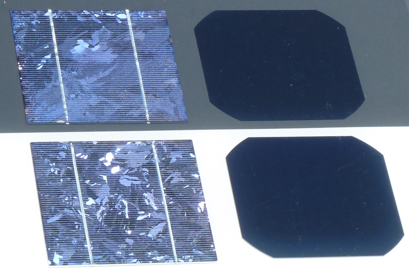
Because ultra-pure silicon has the best electronic properties there is no wonder that monocrystalline silicon is the most efficient material for solar panels on the market. Monocrystalline solar cells offer more electrical power yield per square foot. It performs great especially in warm weather.
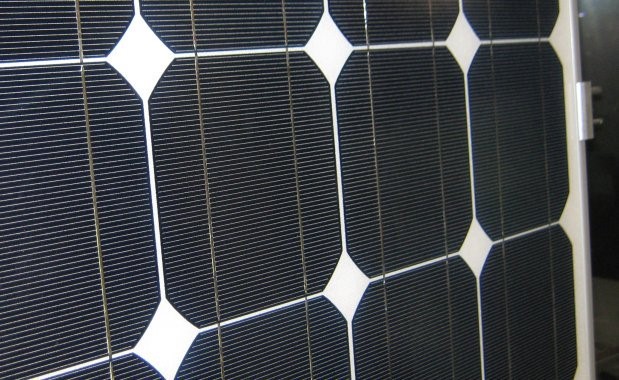
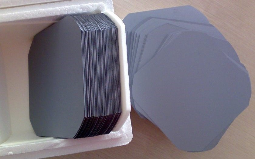
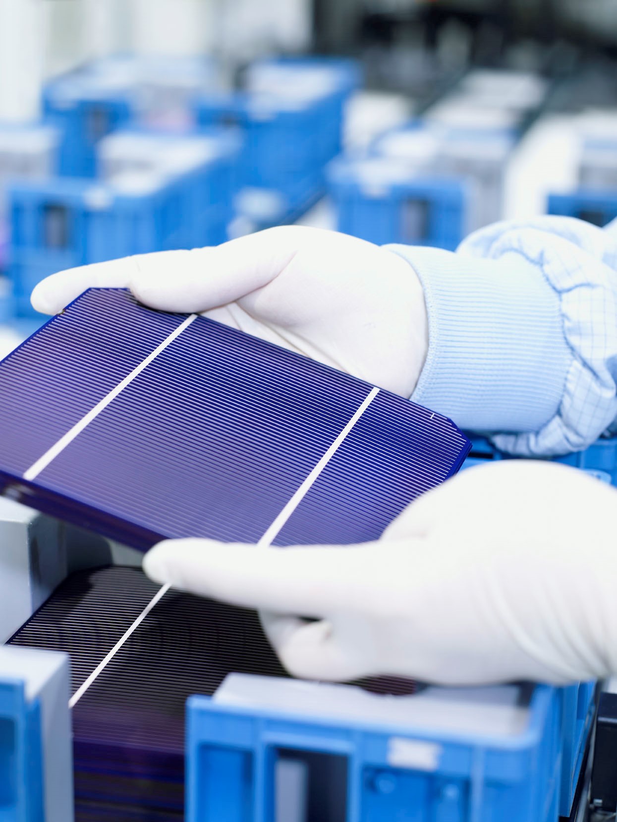
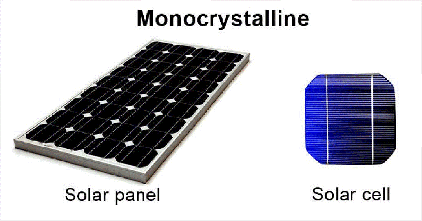
It takes less space than the other kinds of solar panels which makes it perfect for private properties with limited space. Monocrystalline solar panels have characteristic octagonal cells that are arranged closely together.
Monocrystalline solar panels has the longest life (the panels can last up to 25 years) when compared to the other solar panels and that is why its high initial investment for intallation pays off.
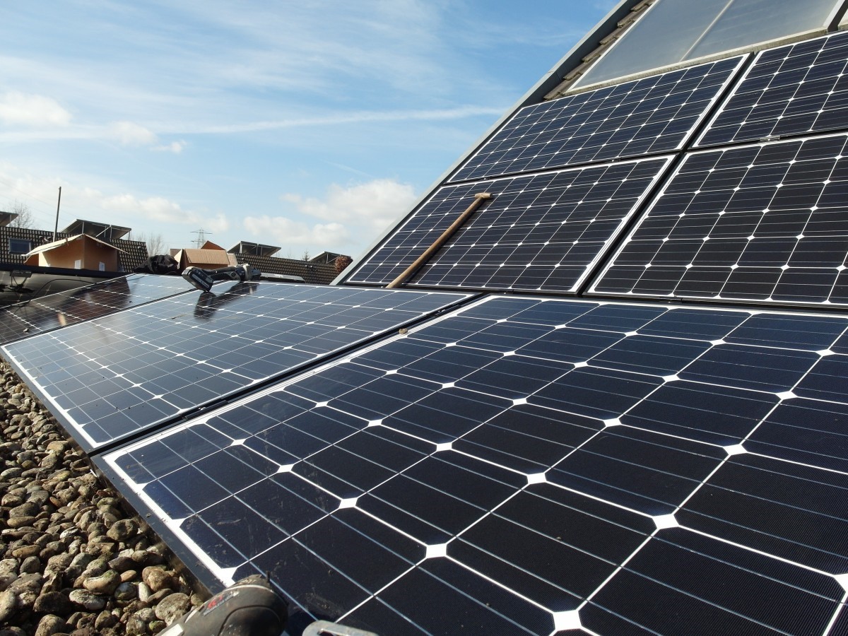
But as at happens with all solar panels monocrystalline silicon solar panels have bad sides too. Its manufacturing process is more costly and takes longer than this of the polycrystalline and thin-film solar panels. This makes it not very affordable option for some home owners who are looking for cheap solar energy technology.
Another downside of monocrystalline silicon solar panels is that they don’t perform really well in shady or snowy spots or places are hidden from the sun and where the sunlight doesn’t reach the surface of the solar panel directly.
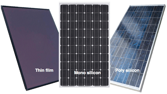
Although it has excellent performance in warm weather, when the temperature goes higher, the performance of the monocrystalline solar panel equally falls. Despite this, monocrystalline solar panels still yields more power in low-light environment in comparison to polycrystalline and thin-film solar panels.
So, our choice of type of solar panel should be determined by the goals of our solar project.
How are monocrystalline silicon solar panels born?
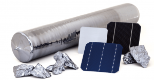
Monocrystalline silicon is a necessary element to produce top quality electronics and for devices that transform effectively the sun’s energy into electrical energy.
The production of monocrystalline silicon is more complicated process compared to the production of other popular types of solar panels made from silicon. Monocrystalline silicon is made by several methods. They include the melting of semiconductor-grade silicon which is in its purest form. This means that it contains only really low percent of impurities (only a few parts per million).
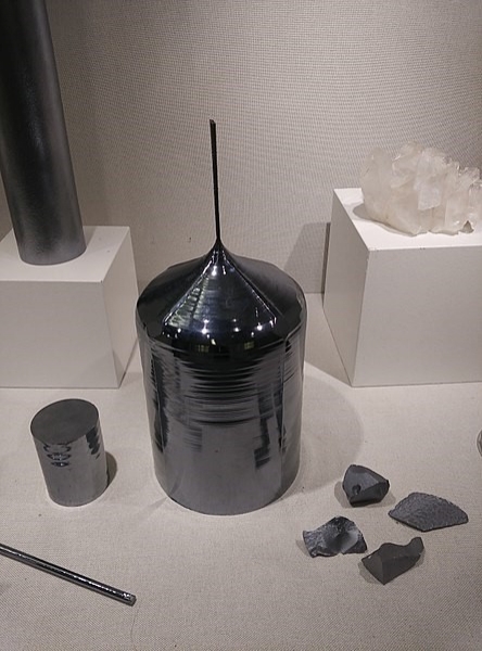
Special processing is needed for creating highly pure silicon (the silicon content must be 99.9999% ). It includes the use of rod-mounted silicon seed crystal with a solid structure which has precise orientation. It is dipped into a molten silicon in a crucible and then with a slow speed brought upwards and quickly rotated.
The rotation and the pulling movement happen at the same time. This helps the pulled material to harden and form into a cylindrically-shaped monocrystalline ingot. The ready cylindrical crystal is called boule.
After the silicon melting procedure, the second step is that we start the formation of a single unbroken crystal by using a seed. It’s a seed crystal – small in size single crystal or polycrystal material mainly used for the replication of a material. It’s used to create large crystal that is going to be grown in a laboratory which is made from the exact same material.
Since seed crystal increases material growth, it avoids the slow and irregular natural process of crystal growth. It allows us to replicate quickly material to meet the industry’s requirements.
The growth of the biggest crystal can be increased by two ways:
- The first method is when we dip the seed in a supersaturated solution and in a molten material which is with cool temperature.
- The second – when we stimulate the growth on the seed face when we pass the material’s vapor over it to grow.
The manufacturing procedure of monocrystalline silicon happens in inert crucible like this of quartz and in inert atmosphere like this of argon. The reason for this is to prevent getting impurities that will have negative influence on the uniformity of the crystal.
Czochralski method
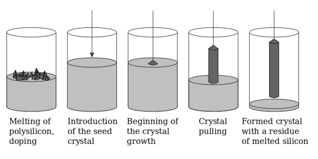
The most popular method for producing highly purified monocrystalline silicon is Czochralski method (or CZ in short). This method is the most commonly used for the biggest part of silicon production for commercial purposes. It had a considerable contribution to the overall development of solar panels manufacturing industry.
It bears the name of a Polish scientist. As it often happens with most great discoveries, the scientist discovers this method by accident. Once while working in his laboratory Czochralski dipped his pen by accident into molten tin substance instead in the liquid ink.
The method of Czochralski sacrifices the silicon’s purity to a certain extent. Despite this fact, this method for crystal growth offers many benefits such as increased resistance to thermal force for the solar panels, increased speed of the manufacturing process and considerably low price friendly to the majority of customers.
What is float-zone growth?
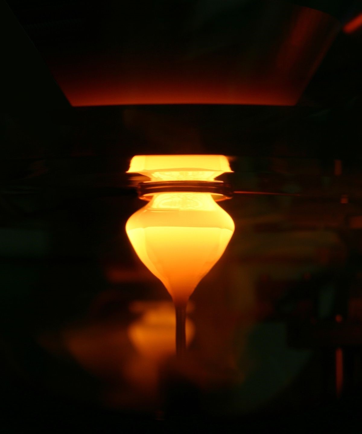
In order to regulate and slow down the dynamic flow magnetic fields are used. This improves the crystallization’s uniformity even more. There is a second method to do this and it’s called float-zone growth. The silicon made by this method goes through a vertical zone melting. The result from this process is also silicon of the purest quality.
It includes polycrystalline silicon rod which goes through a radiofrequency heating coil. This creates a concentrated molten zone. From this zone the crystal seed ingot starts to grow. This method is applied mainly for the production of detector applications and power devices.
The disadvantage of this method is that the wafers have a limited size – 150 mm. because of the limited surface tension during the growth process.
The Bridgman method
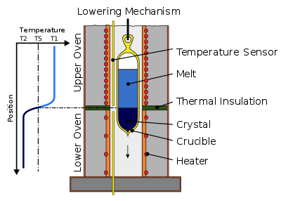
Another way of achieving crystal growth – the Bridgman method. It involves two almost similar to one another methods for producing silicon boules. This method includes the movement of the crucible through a temperature gradient in order to make it cooler from this end of the crucible that contains the seed. It can be used to harden both monocrystalline ingots and polycrystalline ingots. After this the hardened ingots are also cut by a diamond saw into wafers of equal size designed for the construction of solar panels.
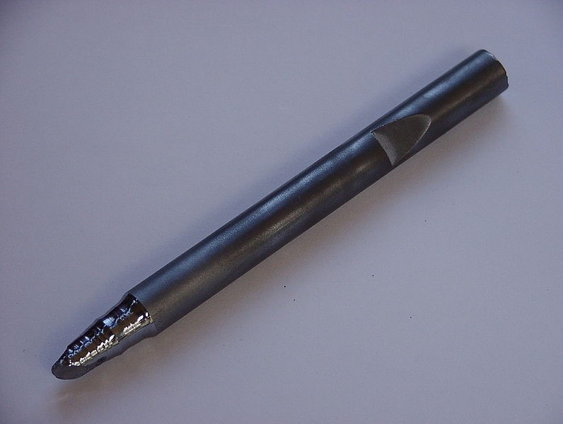
During this phase the temperature of the molten silicon is constantly controlled. The ready silicon boule is 1 to 2-metre long and it weighs several hundred kilograms. The silicon wafers cut from this boule usually have a diameter of 75 to 200 mm. but hey can be made with a diameter of 400 mm.
The standard silicon boules for commercial purposes are 300 or 200mm in diameter. By this method a solid block of silicon is made with just one crystal which gives the name of the silicon - monocrystalline. The end-product of the method, which is monocrystalline silicon, has the most pure quality.
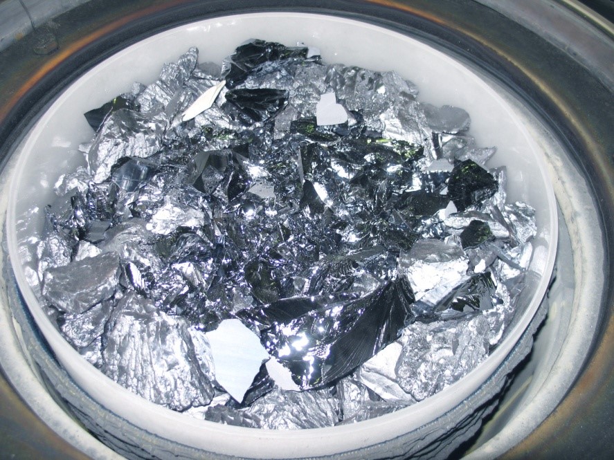
After the silicon block is formed, it’s cut until it has a square form which is the reason why this production method produces so much silicon waste. The next step is cutting the square silicon into wafers of the same color. Their thickness is 0.2 to 0. 75 mm.
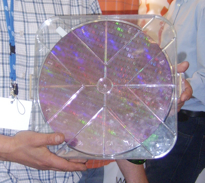
The cut wafers are polished until the desirable level of flatness is achieved. For integrated circuits they are made completely flat and for the purpose of solar cells production they are made to be with a textured surface. They are afterwards arranged in the standard pattern of all monocrystalline solar panels.
Why we should add impurities to the silicon for solar panels?
The silicon’s usefulness in the production of electronic devices is achieved by the addition of impurities. Due to the fact that in the production of solar cells there are less severe regulations concerning the imperfections in the material’s structure in comparison to the more strict regulations on microelectronics manufacturing. Therefore we can use solar-grade silicon of low grade for making solar cells and make a compromise with the level of purity of the silicon’s structure.
However, the production of monocrystalline silicon solar panels reaped many benefits because of the improvement in the monocrystalline production’s speed for the needs of the electronics manufacturing.
When we add just a small amount of impurities to the silicon during its manufacturing process this changes its electrical characteristics. These industrially added impurities are called dopants.
The whole process of adding dopants goes by the name doping. The amount of dopants added to the silicon is equal to one part in 100 million. Even though we add impurities to the silicon’s structure, the crystal lattice of the silicon is created in the right way.

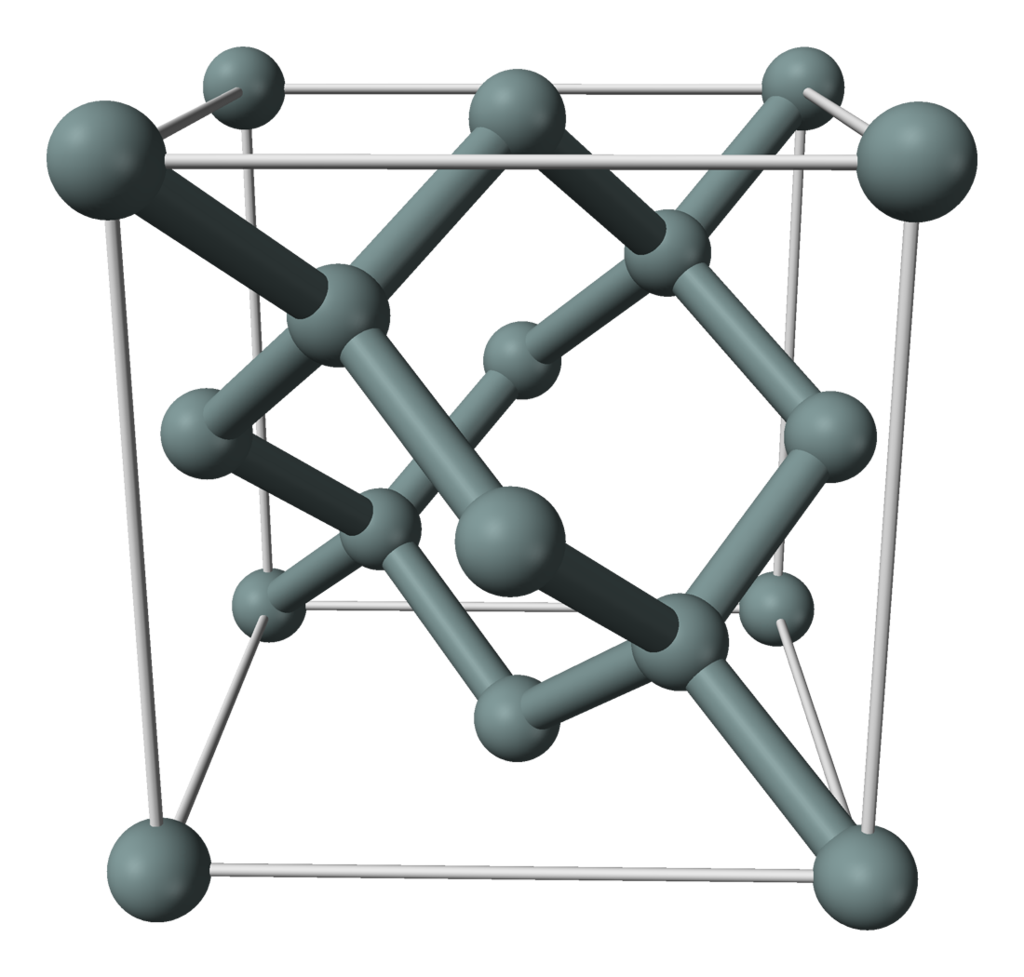
Highly pure silicon doesn’t conduct electricity but acts like an insulator. Every silicon atom contains four electrons in its exterior shell. Each silicon atom shares its four electrons with four other silicon atoms. These atoms form a compacted crystalline structure which is a diamond cubic.
There all the electrons are kept stable in one spot. Because there are not free electrons in the silicon’s structure to play the role of charge carriers, the purest grade silicon has excellent insulating abilities.
